Advanced Technical Ceramics, Precision Alumina, Silicon Carbide, Crucible Parts



News
What Properties Make Boron Nitride Suitable for Semiconductor Manufacturing?
1. Introduction In boron nitride semiconductor manufacturing, ceramic materials are exposed to a combination of high temperature, thermal cycling, vacuum, reactive gases, electrical fields, and extremely strict contamination requirements. Under these conditions,…
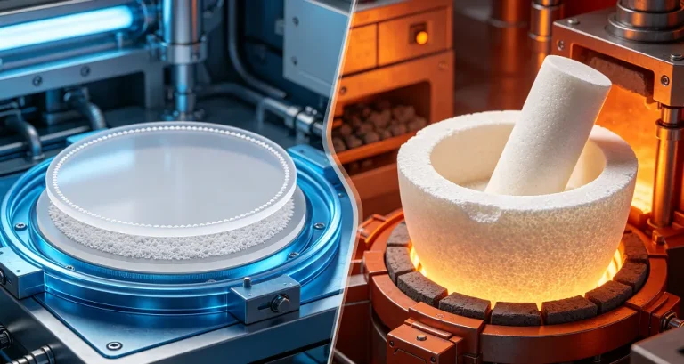
9 Boron Nitride Applications in Semiconductor Manufacturing Engineers Should Know
1. Why Boron Nitride Matters in Semiconductor Manufacturing In advanced boron nitride semiconductor manufacturing applications, material selection is rarely determined by a single property such as maximum temperature or dielectric strength. Semiconductor…
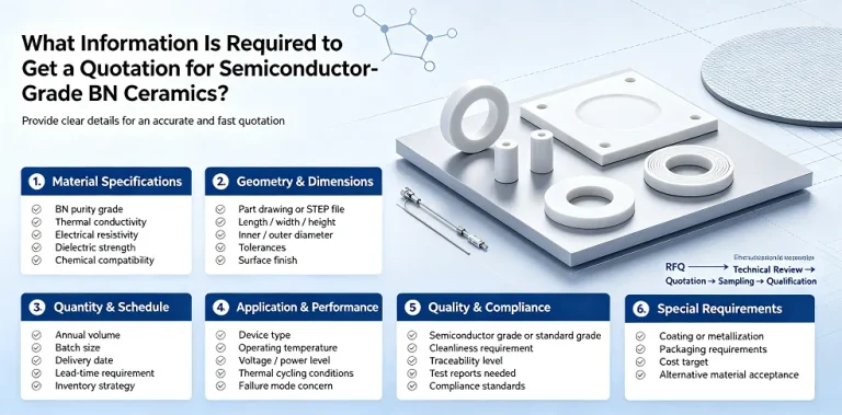
What Information Is Required to Get a Quotation for Semiconductor-Grade BN Ceramics?
Obtaining a quotation for semiconductor-grade boron nitride ceramics is fundamentally different from requesting a price for a standard machined ceramic part. In semiconductor equipment, the cost of a BN component is determined…
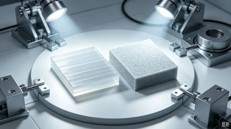
How to Custom Manufacture Boron Nitride Insulator Rings, Gas Nozzles, and Wafer Chuck Parts?
Engineering Considerations for Custom Boron Nitride Components In semiconductor and high-temperature processing equipment, standard ceramic components are often unable to fully satisfy the requirements of complex thermal structures, precision positioning systems, and…
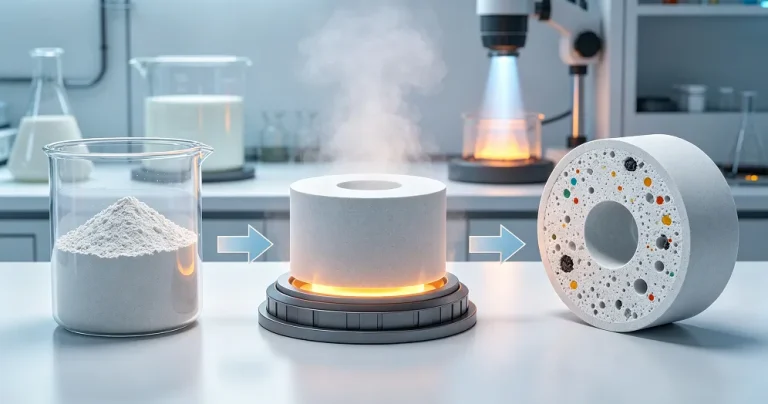
What Binders or Impurities in Boron Nitride Ceramic Can Contaminate Silicon Wafers?
Why Contamination Control Matters for Boron Nitride Used in Semiconductor Equipment In semiconductor manufacturing, every material placed near a silicon wafer must be evaluated not only for thermal stability and mechanical performance…
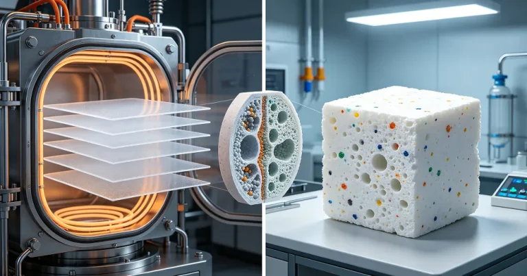
How to Ensure Low Outgassing and High Purity in Semiconductor-Grade Boron Nitride?
Why Purity and Outgassing Control Are Critical for Semiconductor-Grade Boron Nitride In semiconductor equipment, ceramic components are not simply passive structural materials. Every material placed inside a vacuum chamber, high-temperature furnace, deposition…
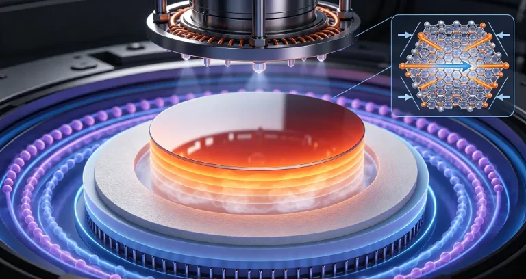
How Does the Anisotropy (Directionality) of Boron Nitride Affect Thermal Conductivity in Chip Equipment?
Understanding the Directional Thermal Behavior of Boron Nitride in Semiconductor Equipment In advanced semiconductor equipment, thermal management is no longer only a question of selecting a material with high thermal conductivity. As…
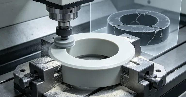
Is Boron Nitride Machinable to Tight Tolerances for Semiconductor Parts?
When engineers specify ceramic components for semiconductor equipment, “machinable” is not enough. The real question is whether the material can be processed into the required geometry, dimensional tolerance, surface condition, flatness, concentricity,…
Which Boron Nitride Grade Is Best for MOCVD/CVD Crucibles and Wafer Applications?
In semiconductor processing, asking which boron nitride grade is “best” for MOCVD/CVD crucibles or wafer-related components is not simply a question of selecting the highest-purity BN available. The correct engineering choice depends…
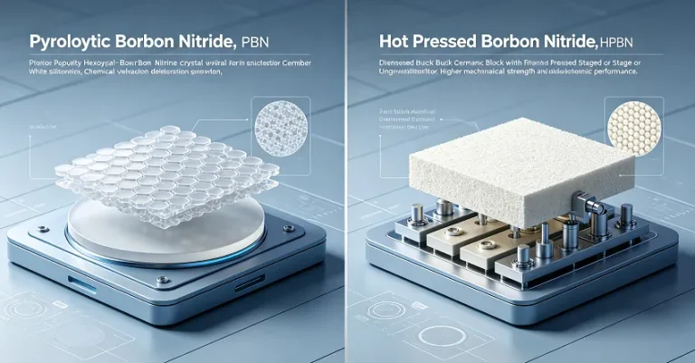
What Is the Difference Between Pyrolytic Boron Nitride (PBN) and Hot Pressed Boron Nitride (HPBN) in Chip Fabrication?
As semiconductor fabrication moves toward tighter process windows, higher operating temperatures, and stricter contamination control, ceramic components inside process equipment have become increasingly important. Materials used near wafers, epitaxial layers, heaters, plasma…
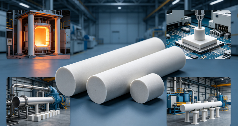
Why Is Boron Nitride Used in Semiconductor Manufacturing?
Semiconductor manufacturing places unusually demanding requirements on the materials used inside thermal-processing, vacuum, deposition, insulation, and plasma equipment. A component may be exposed to high temperature, rapid thermal cycling, electrical fields, vacuum,…